Barry L. Kramer Engineering Services
|
Barry L. Kramer Engineering Services
|
|
Products — PCI Bus Extender and Interface Board This board is a multi-purpose passive 5-volt, 32-bit Conventional PCI 2.0 through 2.3 card designed to interface a motherboard to test equipment (such as logic analyzers, oscilloscopes, and current meters) for debugging, product validation, and reverse engineering. It can be used by itself as a cost-effective PCI interface or extender ("riser") card, or accept a Device Under Test in the upper slot, supporting the isolation of the most common PCI signals from the motherboard with disconnect switches supporting new peripheral design development. Four 16V8 devices can be installed for special prototyping or debug support such as "Using Delayed FRAME# to Differentiate Address Phases." The Product Manual contains details on the product features and usage and is available for your convenience. Note: This is a legacy device: Conventional PCI version 2.2, 5-volt only card, for performing analysis in older systems. Unmodified, it is not keyed for a 3.3-volt-only conventional PCI motherboard slot, and it is not PCI Express (which is a serial bus, not parallel like this device). It accepts universal (mixed 5V/3.3V) cards in the upper slot and does supply 3.3V to the upper connector when the fuse F2 is installed. Product images are available below.
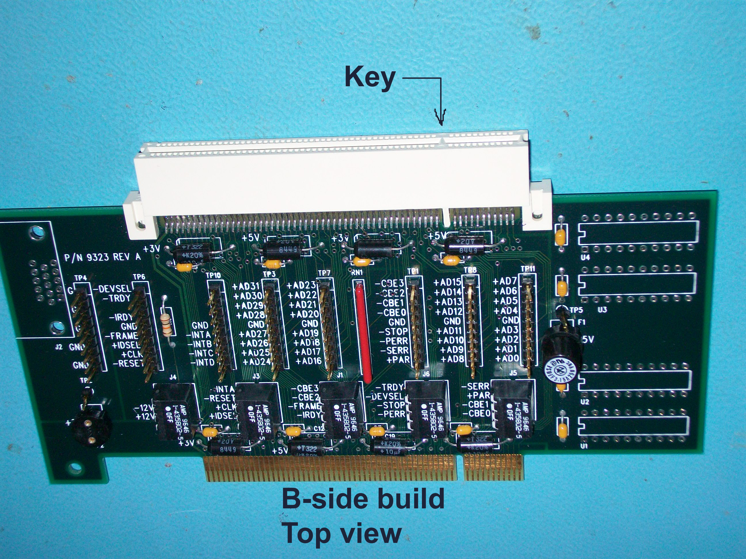
A Note About Component Builds This board is a reversible design. Inspect your system configuration to determine which side of the board you want the isolation switches, headers,and test points mounted in relation to the backplate (card bracket) and key, especially if you are working with a system using a riser card or limited space between boards. Here is a useful reference: http://en.wikipedia.org/wiki/File:PCI_Keying.png#file I am currently investigating modification options of
this card for use in a 3.3V motherboard environment.
The A-side component bulid provides isolation switches and test points mounted on the surface of the board that faces you when the backplate (mounting bracket) is on your right, and the key notch is on your left. Click for larger images
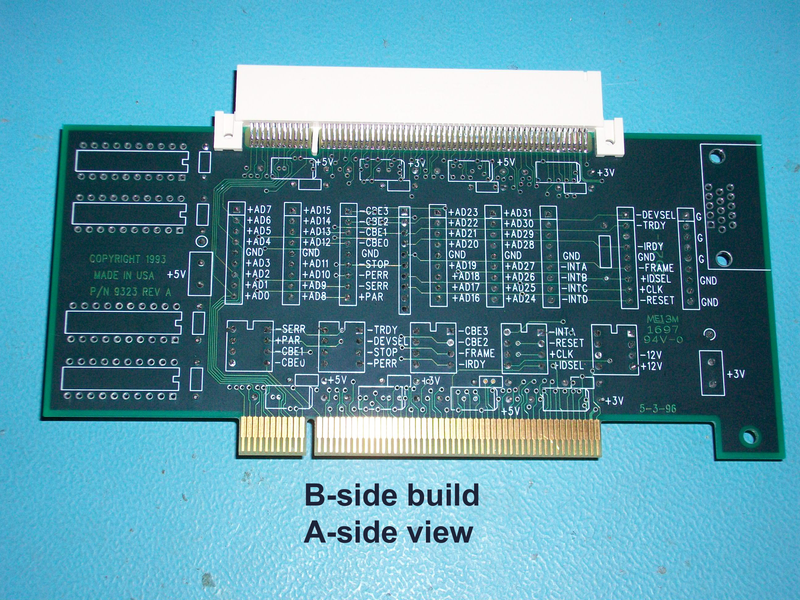
Product Images — B-side component build (click for larger images) The B-side component bulid provides isolation switches and test points mounted on the surface of the board that faces you when the backplate (mounting bracket) is on your left, and the key notch is on your right. Click for larger images
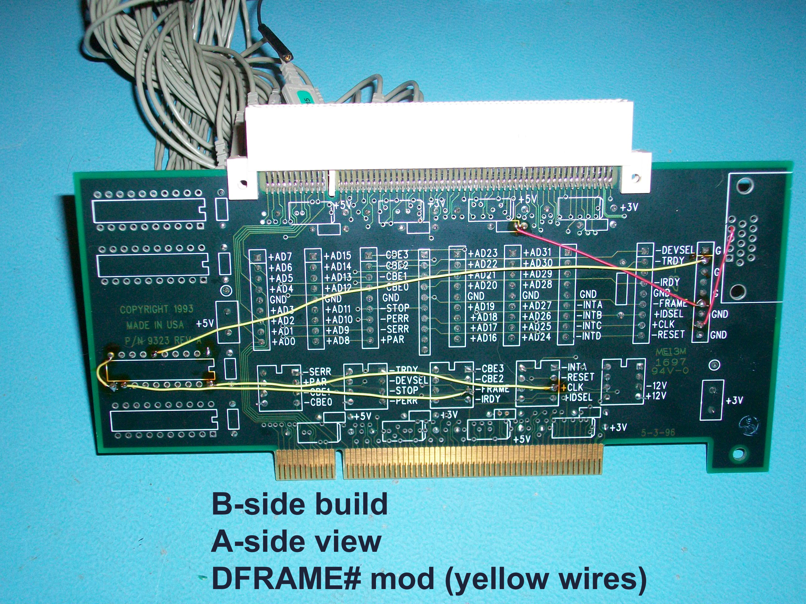
The following is the B-side and A-side view of a B-side-component-build board, modified with the DFRAME# circuit and wired up to three 16555A pods of an HP 16500C logic analyzer. It looks messy but only takes about 10 minutes to wire up. The yellow wires are the DFRAME# modification. The pink wires are to bring the REQ# and GNT# signals out to test points. Click for larger images
Here is one more example of a (different) 5V-only PCI board with a B-side component build: http://en.wikipedia.org/wiki/File:32-bit_PCI_card.JPG
For more information, refer to the Conventional PCI pinout specification on Wikipedia, or the actual PCI specification. The Wikipedia article visually demonstrates the differences between the 5V and 3.3V keyings, and the pinout is clearly and conveniently referenced looking down into the motherboard connector.
Pricing Order inquiries may be sent by email. $275 for one unit, Customers will receive schematics, layouts, and a recommended logic analyzer wiring configuration with their purchase. For an additional $50, I will
modify your board to generate a delayed FRAME#
output which can be used to differentiate Address from Data phases in
PCI transactions. State listings can then be set up to exclude all wait
states, or further qualified to store only particular transaction types.
This is excellent for timing software operations or hardware events, for
determining burst lengths or merge behavior, and for comparing performance
of time-critical software implementations for device drivers for PCI devices.
Competing products and comparison This product is not the only option for performing PCI bus analysis. The following chart provides some detail about the differences between the 9323A board and some competing products:
|
| Layout and design copyright 2012 Barry L. Kramer. All rights reserved. |